2. OpenSourceSDRLab LibreSDR
This page showcases measured performance for a LibreSDR I bought from OpenSourceSDRlab on Aliexpress.
The original seller link would be: https://opensourcesdrlab.com/products/libresdr-zynqsdr-ad9363-zynq7020
The package received contains:
1x SDR device in antistatic Bag
2x USB-C cables
1x ethernet cable
1x Allen key
1x USB-A to USB-C adapter
4x antennas
1x blank 32GB micro-SD card
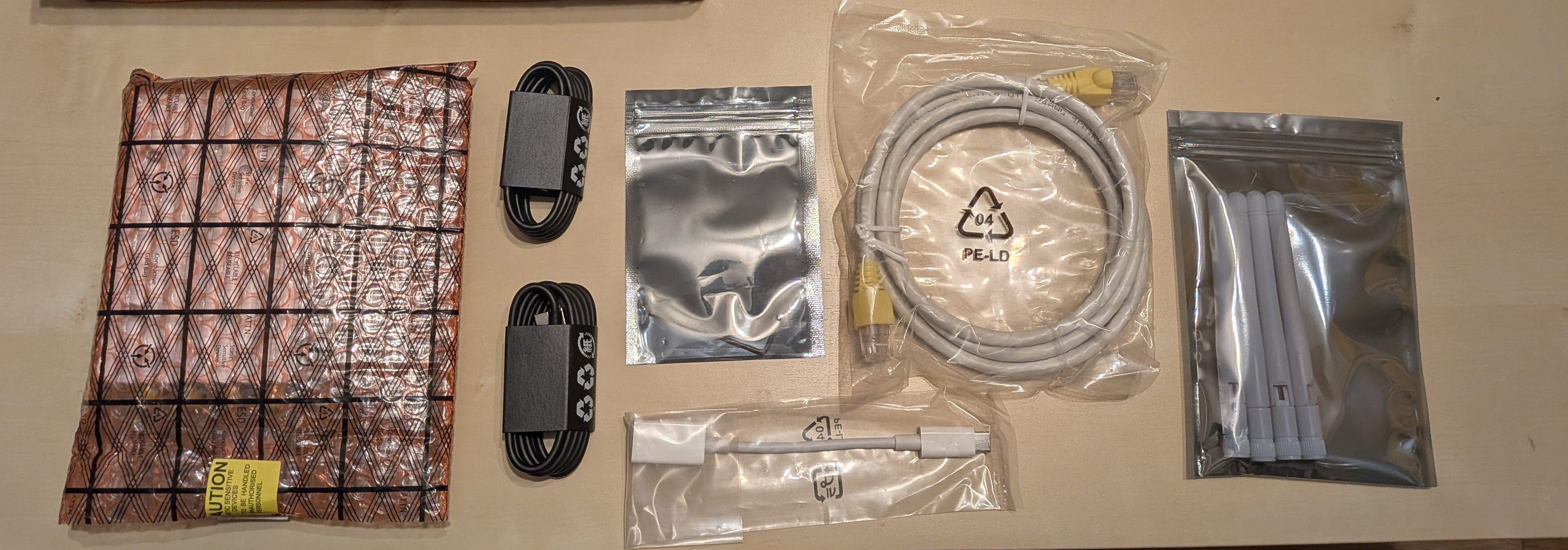
Box content
It can be bought in a variety of places such as Ebay, Aliexpress, Banggood… and of course the official seller’s own website.
2.1. Hardware
Feature |
Description |
|---|---|
FPGA |
XC7020-2CLG400I with 2-core Cortex A9 |
RAM |
1GB 32bit wide DDR3 1066MHz |
Flash |
32MB QSPI, also support micro SD card |
RFIC |
AD9363 (Can be “hacked” to AD9361 or AD9364) with 2 Transmit + 2 Receive channels |
ADC/DAC resolution |
12 bits |
Max Sampling rate |
61.44 Msps |
Max bandwidth |
20 MHz (AD9363 mode) or 56 MHz (AD9364/61 mode) |
Frequency range |
325~3800 MHz (AD9363 mode) or 70~6000MHz (AD9364/61 mode) |
Clock |
VCTCXO 40MHZ 0.5ppm, with external clock input |
Connections |
USB 2.0 OTG + USB debug (Serial) + Gigabit ethernet. USB connectors are Type C |
As far as I know the current/latest PCB revision is “rev5”. Schematics can be found here
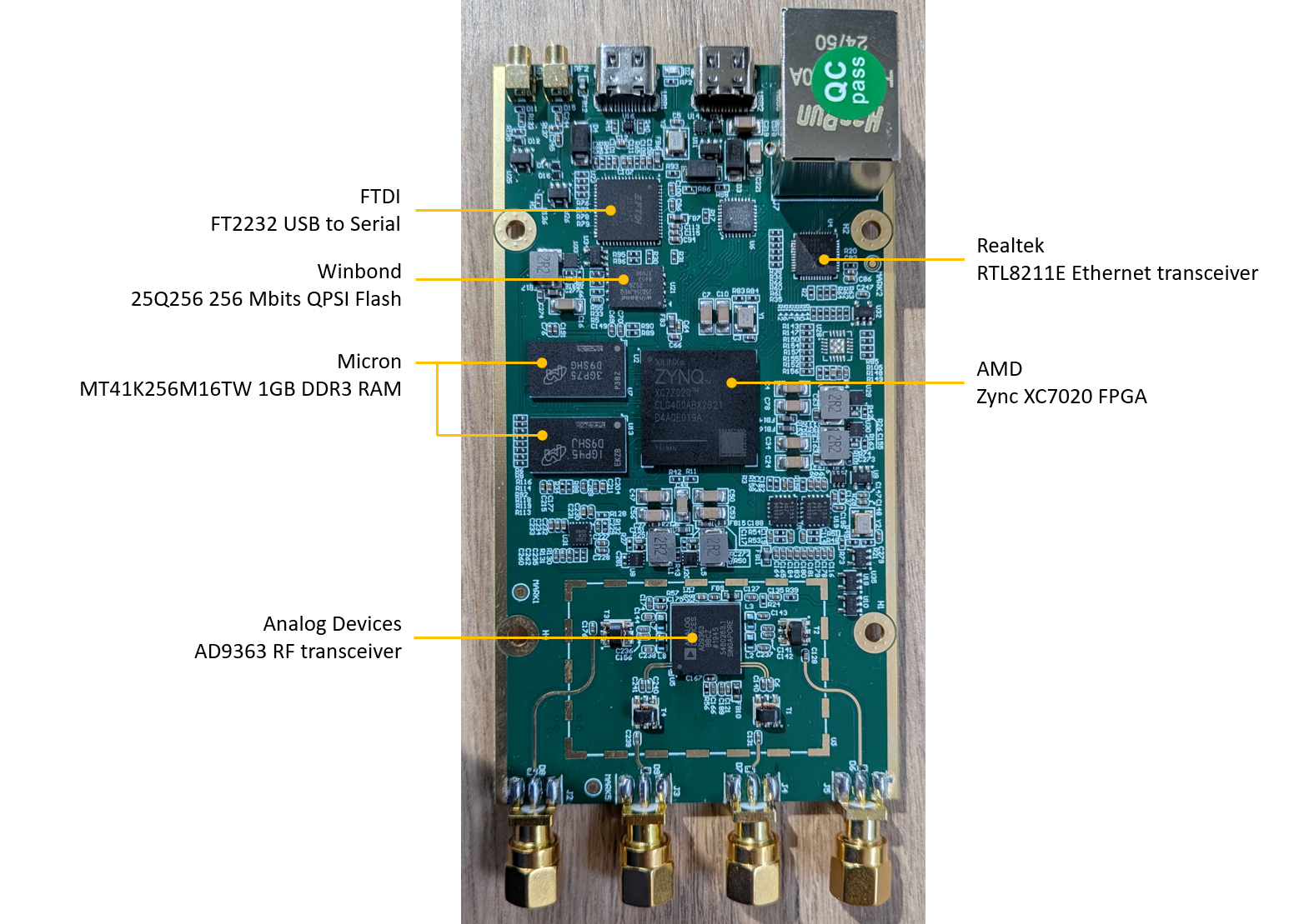
LibreSDR typical PCB
Caution
There are multiple sources/manufacturers, some official and some not. The alleged original designer “jiskra” mentions on this thread that some knock-offs exist that use 2nd-hand ADI chips, i.e. chips that were pulled from other products, reballed, and reused.
He mentions that the devices provided by OpenSourceSDRlab should be original ones
Users have reported that some versions seem to have no stiching vias. This is the case of the Hamgeek version for example. The vias appear to be there if we look closely, but the surface coating (resist, finish) seems te be very thick and covering them to the point where we do not see them anymore.
There are two main casing variants: one with “vertical” stripes in the aluminium shell and one with “horizontal” stripes. This can be seen here. Markings/engraving also exists in different flavours. The case marking of my device matches the one shown by sq6emm here.
My device has the marking “LibresDR” (lowercase “s”) and stiching vias are clearly visible on the PCB:
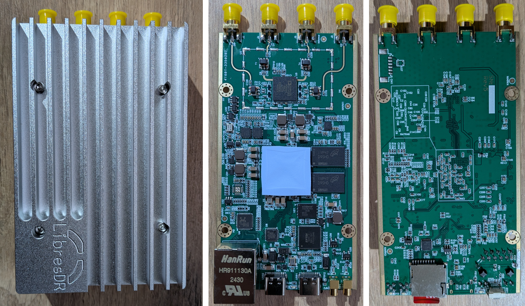
Casing and PCB of OpenSourceSDRLab device
Performance data given below is for the default configuration of my device (as I received it):
AD9363 mode (325-3800MHz / max BW 20MHz)
1RX + 1TX
All tests:
Are conducted using the USB connection. This would NOT affect high-bandwidth measurement as IQ data was taken as “one-shot”, not continuous streaming.
Have setup cable loss deembedded from the measurement: the reference plane is the device’s SMA connector
Note
I have also tested the Hamgeek version but my Hamgeek device, acquired through Banggood, seems to have an issue. It works but some key metrics appear to be really bad. I will give them the benefit of the doubt and assume I just got a faulty device, and therefore will not report what I measured on this website.
2.2. Firmware
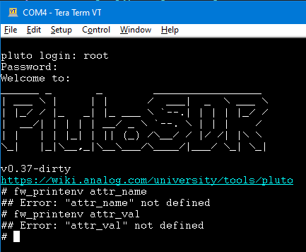
My devices came with a default firmware dubbed “v0.37-dirty”.
The firmware:
Is in “AD9363” mode, ie limited to the standard frequency range of 325-3800MHz / 20MHz bandwidth
Default RF mode
Is configured in 1TX-1RX only (so TX2 and RX2 port unusable)
Has ethernet enabled by default (some forums seem to say this is not the case but it was on mine):
Ethernet configuration
Note
At the time of writing I have not tested ethernet yet, only USB
2.3. Typical test setup
The typical test setup is simple: the port under test is connected to the test instrument with an RF cable, and a 6dB attenuator is placed at the device’s SMA connector to tame any mismatch introduced by the RF cable.

Typical test setup
Setup cable loss has been characterised and is removed from the test results.
2.4. Port impedance
Test conditions:
Configuration |
RF port |
TX1 or RX1 port enabled |
||
Sampling rate |
1Msps |
|||
Tx Gain |
0dB |
|||
Rx Gain |
70dB |
|||
LO |
1GHz |
|||
Parameter sweep |
None |
|||
The TX or RX port is connected to a VNA and S11 is measured

Port impedance setup
Test results:
From the plots we can see that
RX S11 looks OK between 800 - 2500 MHz
TX S11 looks OK between 250 - 2000 MHz
2.5. RX tests
2.5.1. Rx Frequency response
This test measures the frequency response of the receive chain
Caution
There are 3 frequency ranges defined in the Analog Devices documentation, each with a different RX gain table:
RX LO |
Min GAIN |
Max Gain |
|---|---|---|
70 … 1300 MHz |
-1 dB |
73dB |
1300 … 4000 MHz |
-3 dB |
71 dB |
4000 … 6000 MHz |
-10 dB |
62 dB |
Test conditions:
Configuration |
RF port |
RX1 |
||
Sampling rate |
1.024 Msps |
|||
SG level |
-15/-20 dBFs @ gain = 0dB |
|||
Tone frequency |
LO+100kHz |
|||
Rx Gain |
0 dB |
|||
Rx buffer size |
2048 |
|||
Parameter sweep |
Rx Gain, LO frequency |
|||
Initial condition:
The signal generator is set to transmit a tone at LO+100kHz
The signal generator level is set to get circa -20dBFs at the receiver with a gain of 0dB (ie very strong but not so strong that we saturate the rx)
Sweep:
At the start of each new frequency range: The dBm scale is calibrated using the 1st frequency of the active frequency range
Sweep frequency and at each step the RX level in dBm is measured, using RSSI
Note
The final result is normalised to the level of the very 1st frequency
Test results:
Only two gains were measured: min and max to check if there was any dependency.
The frequency response looks very similar with both gains
There is significant rolloff after ~2500 MHz, consistant with the S11 response
The response roughly tracks the RX S11 where
S11 is good until 2500 MHz, and frequency response is somewhat flat.
Then S11 degrades and reaches its worst point at around 3500 MHz, which corresponds to the lowest point on the frequency response.
Past 3500 MHz S11 improves slightly again and the frequency response starts going up slightly again.
2.5.2. Rx Gain
This test measures the Gain of the receive chain. What we report is the gain error: it shows us gain linearity at the same time.
Test conditions:
Configuration |
RF port |
RX1 |
||
Sampling rate |
1.024 Msps |
|||
SG level |
-80dBFs @ gain = 0dB |
|||
Tone frequency |
LO+100kHz |
|||
Rx buffer size |
2048 |
|||
Parameter sweep |
Rx Gain, LO frequency |
|||
Initial condition:
The signal generator is set to transmit a tone at LO+100kHz
The signal generator level is set to get circa -80dBFs at the receiver with a gain of 0dB
Sweep:
Sweep gain, RX level in dBFs is measured using an FFT at each step
The Gain error for each step is found by comparing level measured at Gain G vs level measured at Gain 0dB
Note
The final result is normalised to the gain of 0dB
Test results:
The Gain Error remains relatively small across the whole gain range and across frequency.
There is a global tendancy for gain error to increase (somewhat) linearly with requested gain: this means that the gain is not quite linear.
2.5.3. Rx Bandwidth filter response
This test measures the frequency response of the baseband filter that sets the bandwidth
Test conditions:
Configuration |
RF port |
RX1 |
||
LO |
1000 MHz |
|||
SG level |
-20dBFs @ gain = 0dB |
|||
Tone frequency |
LO+100kHz |
|||
Rx buffer size |
2048 |
|||
Sampling rate |
min(3*BW, 30) MHz |
|||
Parameter sweep |
Rx Bandwidth |
|||
Initial condition:
The signal generator is set to transmit a tone at LO+100kHz
The signal generator level is set to get circa -20dBFs at the receiver with a gain of 0dB
Sweep:
While the signal generator frequency is kept constant, the RX LO is swept across the entire bandwidth of the filter (and a little more)
Measurement is done in dBFs using an FFT at each step
The FFT bin where the tone is expected is computed, and tone level measured
This methodology allows us to get a result that is independent of front-end loss
Note
The final result is normalised to the center frequency of the filter
Test results:
We see an interesting ripple in the filter response. I have checked manually and it is real, not a measurement issue. On wide bandwidths the passband ripple gets quite large, around 1.5dB
Filters at 250 kHz and 300 kHz BW look very similar and are too wide
2.5.4. Rx Spurious Emissions
This test measures the level of spurs that are leaking out of the RX port while active
Test conditions:
Configuration |
RF port |
RX1 |
||
LO |
1000 MHz |
|||
Rx buffer size |
2048 |
|||
Bandwidth |
1 MHz |
|||
Parameter sweep |
None, this was done as a spot measurement |
|||
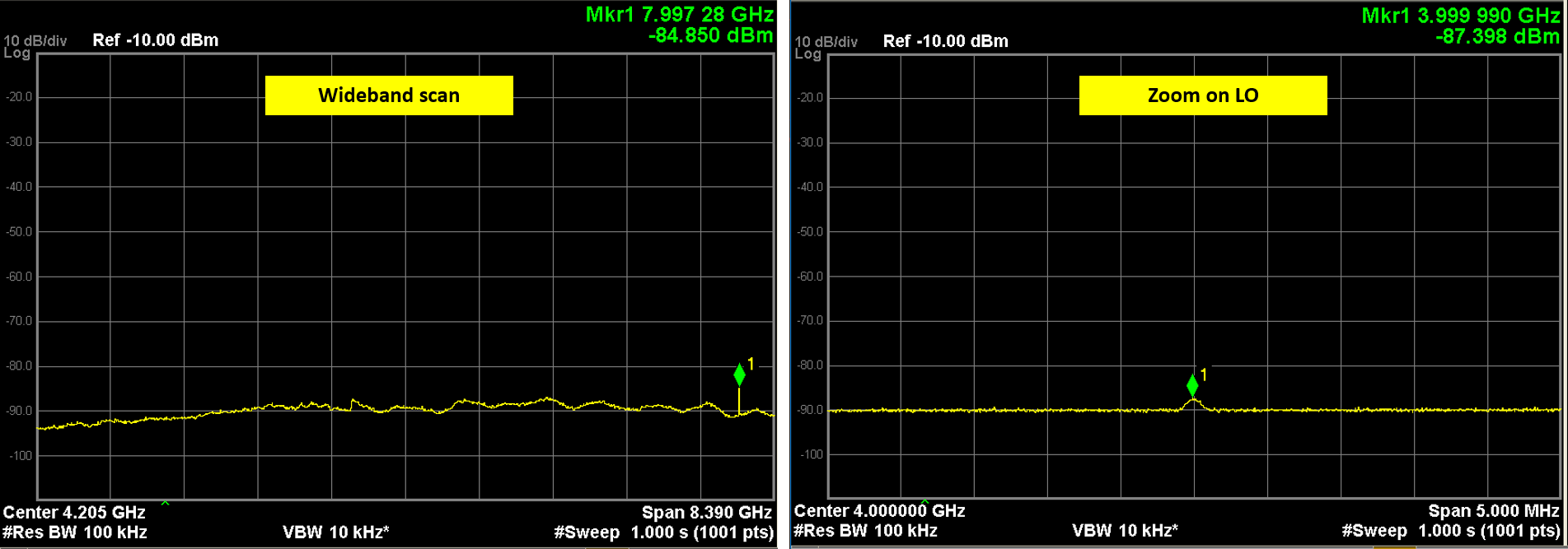
The RX port is connected to a spectrum analyser and measurement is taken from the spectrum analyser.

RX Spurious setup
Test results:
Wideband scan shows nothing except a spur at 8GHz which is 2x the VCO frequency. A zoom on the VCO frequency reveals a tiny spur at approx -90 dBm, so essentially nothing.
2.5.5. Rx Noise figure
This test measures the noise figure of the entire receive chain
Test conditions:
Configuration |
RF port |
RX1 |
||
LO |
1000 MHz |
|||
SG level |
-80dBFs @ gain = 0 dB |
|||
Tone frequency |
LO+100kHz |
|||
Rx buffer size |
2048 |
|||
Rx Gain |
70 dB |
|||
Parameter sweep |
Rx Bandwidth, Rx LO |
|||
By lack of noise source or any specialised equipment, I used the gain method to measure NF. It is theoretically possible since the maximum RX Gain is very high (~70dB), assuming thermal noise dominates. It is a “quick and dirty” method but should yield acceptable results.
The idea is to measure noise power while RX is terminated with 50R at maximum gain, and apply the formula:
Initial condition:
The signal generator is initially set to transmit a tone at frequency RX LO + 100kHz
The signal generator level is set to get circa -80dBFs at the receiver with a gain of 0dB
Sweep: For each frequency,
(Max) Gain and dBm scale are calibrated using the signal generator
Once Gain and dBm scale are calibrated, the signal generator is turned off
The total noise power in dBm at the receiver is measured using an FFT
Finally the NF formula given above is applied
Note
The test has been run with only the RX active
Warning
This test was not run in shielded environment.
Test results:
The results are quire reasonable. For this type of device we should expect between 4-8 dB of Noise Figure, which is exactly what we get. Past 2500 MHz the NF degrades which is in line with S11/Frequency response.
Active TX:
If we activate the TX (turned on but not transmitting), degradation may appear where the TX chain produces spurs that couple on the RX. Below is an example with the TX LO set at 1GHz:
We notice some “discrete” degradations in NF, especially at 1 MHz and 5 MHz bandwidth. To avoid these:
Ideally don’t activate the TX at all (as you can only deactivate by rebooting the board)
Or set the TX LO as far away as possible from the RX LO
If you are actively using the TX at the same time then be aware it might degrade the NF
2.6. TX tests
2.6.1. Tx Frequency response
This test measures the frequency response of the transmit chain
Test conditions:
Configuration |
RF port |
TX1 |
||
Sampling rate |
1.024 Msps |
|||
Tone frequency |
LO+100kHz |
|||
Tx Gain |
0 dB (max gain) |
|||
Parameter sweep |
LO frequency |
|||
Initial condition:
The device is set to transmit a tone at a frequency offset of +100kHz
The device is set to transmit at maximum level and gain
Sweep:
Frequency is swept and TX level in dBm is measured using a power meter at each step
Test results:
The output power level is not great: the max power is around -2dBm and between the minimum frequency 350 MHz and the maximum frequency 3800 MHz there is circa 9dB of variation, down to -11dbm at the lowest point. From the AD9363 documentation I would have expected more than 0dBm
Important
I have tried investigating this poor output power performance following feedback from users found on various websites. I have summarized my findings in Tx power investigation.
The response roughly tracks the TX S11 where
S11 is good below 2000 MHz
Then S11 degrades and reaches its worst point at around 2200 MHz, which corresponds to a trough on the frequency response.
Then S11 improves again around 2700MHz and the frequency response also improves, and after that further degrades
2.6.2. Tx Gain
This test measures the Gain linearity of the transmit chain
Test conditions:
Configuration |
RF port |
TX1 |
||
Sampling rate |
1.024 Msps |
|||
Tone frequency |
LO+100kHz |
|||
Parameter sweep |
LO frequency, Gain |
|||
Initial condition:
The device is set to transmit a tone at a frequency offset of +100kHz
The device is set to transmit at maximum level
A reference measurement is taken at maximum gain
Sweep:
Frequency and Gain are swept, and tx power measured at each step
Gain is computed as difference between current measurement and reference measurement
Test results:
The plots show that the gain is very linear but only from from -70dB to -20dB. Above -20dB gain we start showing a little bit of compression, and below -70dB we can’t backoff enough.
2.6.3. Tx Filter bandwidth response
Not measured, see Rx Bandwidth filter response, I expect the response to be identical
2.6.4. Tx LO leakage and Image
This test measures the LO and Image while transmitting a test tone
Test conditions:
Configuration |
RF port |
TX1 |
||
Sampling rate |
20 Msps |
|||
Tone frequency |
LO + 1 MHz |
|||
Tone level |
-3 dBFs |
|||
Parameter sweep |
LO frequency, Gain, Bw |
|||
Initial condition:
The device is set to transmit a tone at a frequency offset of +1 MHz
The device is set to transmit at maximum level
The sdr sampling rate is set at 20 MHz
Sweep:
Bw, Frequency and Gain are swept
At each step LO and Image are measured using the analyser
Test results:
LO: Values match datasheet for 0dB attenuation but are worse than datasheet at 40dB attenuation by a few dB. Interestingly there seem to be a band specifically around -40dB gain where LO leakage is degraded.
Image: Nothing out of the ordinary, there is a noticeable degradation of image level at higher frequencies
2.6.5. Tx Harmonics
This test measures the transmit harmonics
Test conditions:
Configuration |
RF port |
TX1 |
||
Sampling rate |
1.024 Msps |
|||
Tone frequency |
LO+100kHz |
|||
Tone level |
-3 dBFs |
|||
Tx Gain |
0 dB (max gain) |
|||
Parameter sweep |
LO Frequency |
|||
Initial condition:
The device is set to transmit a tone at a frequency offset of +100kHz
The device is set to transmit at maximum level and gain
Sweep:
Frequency is swept, and harmonics are measured at each step. Fundamental is also measured
Note
my analyser could not measure higher than 6GHz
Test results:
Harmonics are quite low, the signal appears clean:
However, this is inconsistent with a manual measurement I made, depicted below.
Manual inspection:
I was looking at VCO spurs and made a wideband acquisition using a spectrum analyser, here shown for LO = 500 MHz:
Note
Ignore absolute levels, the span is too wide so the readings are inaccurate. The shape matters most.
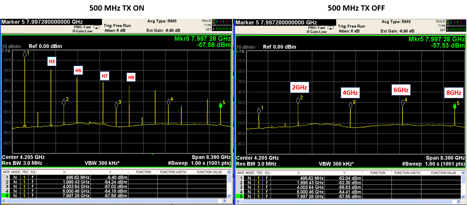
TX spurs at LO = 500 MHz
The picture on the left is with transmitter ON: we see a mix of transmit and VCO harmonics. The picture on the right is with transmitter active but OFF: we see only the VCO spurs. It shows that the VCO runs at 4x the LO frequency, which is quite typical. For an LO of 500 MHz, the VCO would run at 2GHz and its harmonics at 4, 6, 8 GHz and so on: this is exactly what we see on the TX OFF picture.
Problem: on the wideband display, odd harmonics of the test tone (H3, H5, etc) appear to be very high: H3 alone is at -10dBc, not at all what I measured above! Additionally their dBc level does not change regardless of the tone level, which is NOT expected behaviour.
Zooming in manually around each harmonic explains what is happening:

TX spurs at LO = 500 MHz
Since the wanted tone is at \(\text{LO + 100 kHz}\), H2 will be at \(\text{2*LO + 200 kHz}\), H3 at \(\text{3*LO + 300 kHz}\) and so on. This is what was measured previously.
Observation 1:
Picture 4 (2 GHz) shows a strong spur at the center frequency: it’s the VCO fundamental spur, which can easily be mistaken for H4 on a wideband scan. This picture confirms H4 is really low, but the VCO leaks out like crazy. I’ve never seen VCO spurs leaking that much, that to me would point to a PCB layout (ie design, not production) issue.
Observation 2:
Pictures 3 and 5 show why H3 and H5 appear very high on the wideband scan. There are indeed very high spurs but they are NOT H3 and H5! On picture 3 the spur \(IM_a\) appears at \(\text{LO - 100 kHz}\) and on picture 5 the spur \(IM_b\) appears at \(\text{LO + 100 kHz}\): clearly not harmonics, but mixing products of the main tone with something else.
In this case the math is easy to work out: the main tone at 500.1 MHz is mixing with the VCO spur at 2 GHz and so we get two components:
One at \(\text{(2000 + 500.1) MHz = 2500.1 MHz}\): the spur \(IM_b\) we see on picture 5.
One at \(\text{(2000 - 500.1) MHz = 1499.9 MHz}\): the spur \(IM_a\) we see on picture 3
This explains why changing the amplitude of the main tone had no effect on the relative amplitude of the “apparent” harmonics: they were not harmonics.
Danger
This is real. While the spectrum of the tone itself is quite clean, the fact that we have very high VCO leakage and mixing between VCO and tone produces a VERY dirty spectrum. \(IM_a\) will effectively contain 10% of the main tone’s power!
If you want to use this device for transmitting over the air you will need heavy filtering to stay compliant with your local regulations
Back of the envelope calculations:
Assume you add a PA to transmit at +20dBm
The IMa spur would be at +10dBm (assuming PA is perfectly linear and does not compress)
Let’s say spurs > 1GHz must be below -30dBm @ 1MHz MBW (ETSI/RED requirement) -> you want at least 40dB of rejection
Assuming a low-pass filter with a cutoff slightly above our wanted frequency, we’re going to want 40dB of rejection over ~1 octave to secure enough margin on IMa
The filter order to reach 40dB/octave would be ~7! (7*6dB/octave = 42dB)
This is simply not practical, and severely limits the output power one can hope to use.
2.6.6. Tx (baseband) intermodulation
Tx intermodulation was measured manually. The test is meant to show intermodulation products that appear at baseband level due to DAC and other baseband-related non-linearities.
If we transmit a tone at a certain offset \(+ \Delta f\) from the LO, we will of course expect an image at \(- \Delta f\). However, non-linearities in the baseband chain will also cause other spurs to appear. Specifically, in an IQ-based architecture, we will see odd-numbered spurs appearing on alternating side of the LO: if the wanted tone is at \(LO + \Delta f\), we will see a 3rd order IM product at \(LO - 3\Delta f\), 5th order at \(LO + 5\Delta f\), 7th order at \(LO - 7\Delta f\), and so on. Even-order spurs are normally significantly suppressed.
As their order increases, the amplitude of the spurs also decrease rapidly. Usually, only the 3rd and 5th order are prominent/can cause issues in a system
Test conditions:
Configuration |
RF port |
TX1 |
||
Sampling rate |
10 Msps |
|||
Tone frequency |
LO+500kHz |
|||
Tone level |
-3 dBFs |
|||
Tx Gain |
0 dB (max gain) |
|||
Tx LO |
1000 MHz |
|||
Parameter sweep |
None |
|||
Test results:
The spurs are illustrated in the manual measurement below. The span was limited to encompass up to the 5th order spur for better visibility. The highest spur in this example is the 3rd order product, approx. 55dB lower than the wanted tone (good rejection).
We also see two unknown spurs near -100 kHz and +300 kHz, I’m not quite sure what they are since they don’t fall on integers of 100 kHz. Maybe a clock or some fractional signal?

Baseband intermodulation
Unfortunately, since these intermodulation spurs occur at baseband it is not possible to filter them out if they pose a problem. The only way would be to decrease the tone level at the digital stage, before the tone is synthesized by the DAC.
2.6.7. Tx to Rx isolation
This test looks at coupling to the RX port while the TX is transmitting. For this we use a slightly different setup: the TX transmits into a 50R load while we observe the RX port with a spectrum analyser.
Note
This test only looks at TX/RX RF coupling between the SMA and the chip boundary: it looks mostly at isolation on the PCB

TX/RX coupling setup
Test conditions:
Configuration |
RF port |
TX1 / RX1 |
||
Sampling rate |
2 Msps |
|||
Tone frequency |
LO+500kHz |
|||
Tone level |
-3 dBFs |
|||
Tx Gain |
0 dB (max gain) |
|||
Rx Gain |
70 dB (max gain) |
|||
Tx/Rx LO |
1000 MHz |
|||
Parameter sweep |
None |
|||
Test results:
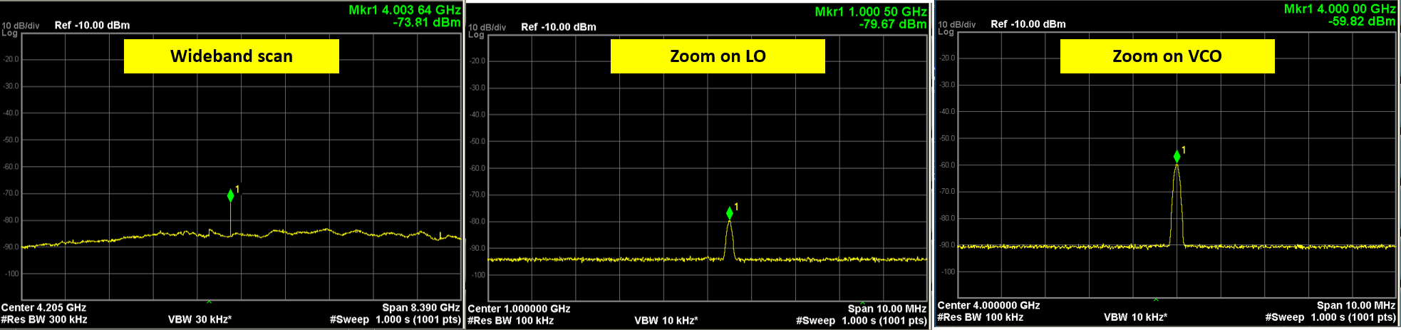
A wideband scan only shows a fairly strong VCO spur. Zooming around the LO frequency, we do see an LO spur but it’s small at approx. -80 dBm. Zooming on the VCO frequency reveals a much stronger spur at approx. -60 dBm, but it’s very far from the LO frequency so would not be an issue in a system.
Focusing on the region around the LO frequency, we have a TX tone at -3 dBm and a spur on the RX side at -80 dBm or an isolation of 77 dB. It is quite clear from this result that most unwanted coupling will occur inside the AD9363, not outside on the PCB.
TRX isolation
2.6.8. Tx power investigation
As seen in Tx Frequency response, the (absolute) output power and the frequency response are not ideal.
Important
I have attempted to investigate it using my (dodgy) Hamgeek device but was ultimately not successful. I only report my findings below for information
I’m currently reluctant to modify my OpenSourceSDRLab device as it behaves reasonably well all things considered. If I decide to modify it later, I will apply the following changes in order:
#4: My PCB has ferrites on all supplies, no 0R mod and this mod is definitely needed for supply stability
#5: Biggest improvement, the TX bias supply was starved
While this will increase power, it was quite clear from my experiments that the RF trace was a big limiting factor. This cannot really be fixed unless you add your own piece of coax between the SMA and balun and disconnect the trace
I have tried the following:
Item |
Description |
Modification and effect |
Trace on plot below |
||
|---|---|---|---|---|---|
1 |
ESD diodes |
Users mention that ESD diode at the output could be the wrong type, with high parasitic capacitance loading the output. However the resulting power loss is > 20dB, not something I see on my device |
Removed diode D6: absolutely no change |
Blue |
|
2 |
Baluns |
Users mention the baluns are poor quality as they are not genuine minicircuits TCM1-63AX+: while this might affect performance at high frequency, it should not affect the output power at low frequency. |
Changed it for a “cheap” TCM1-63AX+ bought on Aliexpress (not an official source): The frequency response changed shape, but no overall improvement |
Red |
|
3 |
RF trace |
A user mentionned that the RF trace between the balun and SMA connector is poor, and replacing it with a piece of coax improved it. |
Connected a pigtail at the output of the balun and it did significantly improve power at high frequency, flattens response. But power is still low overall |
Green |
|
4 |
Ferrites |
Users have noticed that on some of their boards the ferrites on various supply rails have been replaced by 0R links. Indeed, these ferrites seem to have fairly high DCR and are an issue on high current rails. |
Focusing on my TX chain, I replaced the ferrites on the 2V5 (FB4/FB16) and 1V3 rails (FB10/FB11), which power the AD9363: The rails are more stable but no change to output power |
Red |
|
5 |
RF chokes |
The inductors L2/L3 are meant the be used as RF chokes for the TX output bias circuit. They have very high DCR: Once TX was enabled (but not transmitting) the voltage on the TX outputs was measured at 0.9V instead of 1.3V! Given that the quiescent current is around 75mA this is a DCR of 5 Ohms! |
Replaced by BLM18HE102SN1D (I have lots lying around): Increased the output power at all frequencies by 2-3dB, but overall power still low. |
Purple |
|

Modifications
There was unfortunately no magic bullet. The biggest improvements comes from #3 the pigtail (i.e layout limitation) and #5 RF chokes (cheap BOM issue). Combining both these changes would have provided maximum improvement but would NOT have solved the main issue. The rest had negligible impact
I’ve plotted the original frequency response and items 2, 3, 5 above together for comparison. Note that some of the changes are cumulative:
2.7. Conclusion
The device works and has decent performance, there are however two limitations I would highlight:
Minor: The frequency response in both RX and TX could be improved.
Major: TX spurious emissions are really bad owing to huge VCO leakage mixing with transmitted signal.